As USB-C devices continue to demand higher charging power, consumers and businesses alike expect chargers that deliver faster charging without becoming larger or hotter. Traditional silicon-based chargers have served the electronics industry for decades, but their physical limitations become increasingly apparent as power levels exceed 65W.
This is where Gallium Nitride (GaN) technology changes the landscape. By replacing conventional silicon power components with GaN semiconductors, manufacturers can design compact chargers capable of delivering 100W USB-C Power Delivery (PD) while maintaining excellent efficiency and thermal performance.
Today, GaN has become one of the most significant innovations in consumer power electronics, enabling the development of lightweight chargers for laptops, tablets, smartphones, gaming devices, and other USB-C equipment.
This article explains the science behind GaN technology, why it outperforms silicon, and how it is driving the future of fast charging.
Understanding GaN: The Next Generation of Semiconductor Materials
To understand why GaN chargers are smaller, it’s helpful to first examine how power conversion works.
Every charger converts high-voltage AC electricity from the wall outlet into the low-voltage DC power required by electronic devices. During this conversion process, power transistors switch electrical current on and off thousands—or even millions—of times every second.
For decades, these switching devices have been made from silicon.
While silicon remains reliable and cost-effective, it suffers from several physical limitations:
- Higher switching losses
- Greater heat generation
- Lower operating frequencies
- Larger cooling requirements
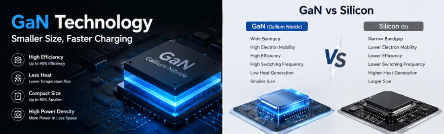
Gallium Nitride, commonly known as GaN, is a wide-bandgap semiconductor material that offers significantly improved electrical characteristics.
Compared with silicon, GaN transistors feature:
- Higher electron mobility
- Lower electrical resistance
- Faster switching speed
- Higher breakdown voltage
- Improved thermal efficiency
These properties allow power supplies to transfer energy more efficiently while wasting less electricity as heat.
Instead of requiring larger transformers, oversized heat sinks, and bulky internal components, GaN designs operate at much higher switching frequencies, dramatically reducing the overall size of the charger.
This is why a modern 100W GaN charger can be nearly half the size of many older laptop power adapters.
Semiconductor Basics of GaN
Although GaN is often discussed in marketing materials, its advantages originate from semiconductor physics.

Wide Bandgap Advantage
Silicon has dominated power electronics because it is inexpensive and easy to manufacture. However, its relatively narrow bandgap limits efficiency at high voltages and high switching frequencies.
GaN has a much wider bandgap, enabling devices to:
- Operate at higher voltages
- Switch much faster
- Generate less energy loss
- Handle higher temperatures
This means designers can build power converters that are simultaneously smaller and more powerful.
Faster Switching
A charger continuously switches current through magnetic components.
The faster this switching occurs:
- The smaller transformers become
- Inductors require less material
- Capacitors shrink
- Overall PCB size decreases
Modern GaN power transistors can switch several times faster than comparable silicon MOSFETs while maintaining high efficiency.
As a result, engineers can reduce internal component size without sacrificing charging performance.
Lower Conduction Loss
Electrical resistance converts energy into unwanted heat.
GaN devices exhibit much lower on-resistance than traditional silicon switches, reducing conduction losses during operation.
Lower resistance means:
- Higher conversion efficiency
- Less wasted power
- Cooler operation
- Longer component lifespan
These improvements become especially important in 100W USB-C PD chargers, where every percentage point of efficiency matters.
Efficiency Improvements Over Silicon
One of the biggest reasons GaN technology has gained industry-wide adoption is its exceptional energy efficiency.
Reduced Switching Losses
Every switching cycle creates a small amount of energy loss.
Since a charger switches millions of times per second, these losses accumulate rapidly.
GaN transistors reduce:
- Turn-on loss
- Turn-off loss
- Reverse recovery loss
- Gate charge loss
Collectively, these improvements can significantly increase total power conversion efficiency.
Many premium GaN chargers now achieve conversion efficiencies exceeding 94–95%, depending on their design and operating conditions.
Less Energy Waste
Higher efficiency means more electricity reaches the connected device instead of becoming heat.
For example:
A traditional charger with 90% efficiency delivering 100W may waste approximately 11W as heat.
A GaN charger operating at 95% efficiency wastes only about 5W.
This reduction improves:
- Charging stability
- Internal reliability
- Energy consumption
- User comfort
Better Performance at High Power
As charging power increases from:
- 20W
- 45W
- 65W
- 100W
- 140W
silicon designs become increasingly difficult to cool.
GaN technology scales much more effectively, allowing manufacturers to build compact chargers that deliver desktop-class power while remaining portable.

Heat Reduction and Size Optimization
Heat has always been one of the biggest challenges in power electronics.
Excessive heat not only reduces efficiency but also accelerates component aging and limits long-term reliability.
GaN technology addresses this challenge from multiple angles.
Smaller Cooling Requirements
Because GaN generates less heat internally, engineers can reduce:
- Aluminum heat sinks
- Thermal pads
- Internal spacing
- Ventilation requirements
These reductions directly contribute to smaller charger dimensions.
Many 100W GaN chargers are now compact enough to fit comfortably into a pocket, replacing much larger laptop adapters.
Higher Power Density
Power density measures how much power can be delivered within a given physical volume.
GaN dramatically increases power density by allowing:
- Smaller transformers
- Compact inductors
- Reduced PCB footprint
- Better thermal distribution
As a result, manufacturers can fit more charging capability into less space.
This enables products featuring:
- Dual USB-C outputs
- Triple-port charging
- Four-port charging
- Intelligent power allocation
without significantly increasing charger size.
Improved Thermal Stability
Lower operating temperatures also benefit long-term reliability.
Electronic components such as:
- Electrolytic capacitors
- MOSFETs
- Controllers
- Transformers
generally last longer when operating at lower temperatures.
High-quality GaN chargers therefore often maintain consistent charging performance over years of daily use.
Manufacturers such as Szjialu incorporate multiple layers of thermal protection, intelligent power management, and certified safety circuitry into their GaN charger designs. Rather than relying on compact size alone, these engineering practices help balance portability, efficiency, and long-term reliability for OEM and ODM customers.
Future of GaN in Power Electronics
GaN technology is still evolving.
While today’s market focuses largely on smartphone and laptop chargers, its applications continue expanding across multiple industries.
Higher Power USB-C Chargers
The introduction of USB Power Delivery 3.1 has expanded USB-C charging up to 240W.
GaN is expected to become the preferred semiconductor platform for:
- 140W chargers
- 180W chargers
- 240W chargers
where silicon designs become increasingly difficult to optimize.
AI and High-Performance Computing
Power-hungry AI laptops and mobile workstations require increasingly efficient charging systems.
GaN enables:
- Smaller travel chargers
- Faster battery replenishment
- Reduced energy loss
- Improved thermal performance
These benefits align well with the growing demand for high-performance portable computing.
Electric Vehicles and Industrial Electronics
Beyond consumer chargers, GaN technology is finding applications in:
- Electric vehicle onboard chargers
- Renewable energy systems
- Data centers
- Telecommunications infrastructure
- Industrial automation
- Medical equipment
Its combination of efficiency, compact size, and high-frequency operation makes it attractive across numerous power conversion applications.
Continued Manufacturing Improvements
As GaN production volumes increase, manufacturing costs continue to decline.
Advances in semiconductor fabrication, packaging technologies, and controller integration are making GaN chargers more affordable than ever.
Industry analysts expect GaN to become the mainstream choice for medium- and high-power USB-C chargers over the coming years, replacing silicon in many premium charging products.
How to Choose a Quality 100W GaN Charger
Not every charger labeled “GaN” delivers the same level of performance. Buyers should evaluate several key factors before making a purchasing decision:
- USB Power Delivery 3.0 or 3.1 compatibility
- Certified safety standards (UL, CE, FCC, UKCA, etc.)
- Intelligent over-current, over-voltage, and over-temperature protection
- Stable output across multiple ports
- High conversion efficiency
- Durable housing materials
- Reliable thermal design
- Proven manufacturing quality
For business buyers, it is equally important to assess the supplier’s engineering capabilities, certification support, production consistency, and OEM/ODM experience, rather than focusing solely on price.
Conclusion
Gallium Nitride has fundamentally transformed modern charging technology. By replacing traditional silicon with a more advanced semiconductor material, manufacturers can build 100W chargers that are significantly smaller, faster, and more efficient than previous generations.
The advantages of GaN extend far beyond compact dimensions. Faster switching speeds, lower power losses, improved thermal performance, and higher power density enable chargers that deliver exceptional performance while maintaining portability and reliability.
As USB-C devices continue to require greater power and consumers increasingly value lightweight, travel-friendly accessories, GaN technology is expected to remain at the forefront of power electronics innovation. Whether developing consumer products or sourcing OEM charging solutions, businesses that invest in well-engineered GaN technology will be better positioned to meet the evolving demands of the global fast-charging market.